


Semi-conductor
Advanced Packaging
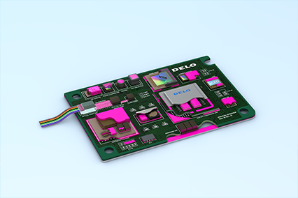
Adhesives are key components in semiconductor-based devices. DELO semiconductor adhesives are used to bond, contact and encapsulate chips and other SMD components on printed circuit boards. DELO has also developed special products for the advanced packaging industry. These help increase package performance.
Wafer-level Micro-optics
Micro-optics and nanostructures are key technologies for the latest miniaturized optoelectronic components in smartphones, smartglasses and vehicles. DELO offers an extensive range of specially adapted adhesives for these requirements.
Bonding of RFID chips
DELO is the world's leading manufacturer of RFID adhesive solutions. Around four out of five RFID labels contain a drop of DELO adhesive. Depending on the process, anisotropic conductive (ACA) or non-conductive (NCA) adhesives are used to bond the chips and satisfy the high requirements demanded of strength, temperature and humidity resistance, and ensure fast processes.
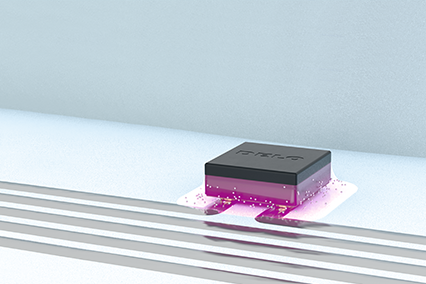
Encapsulation of smart card chips
DELO offers an extensive range of products for smart card modules that covers all requirements necessary for the bonding and long-term protection of chips. It includes various die attach adhesives and encapsulants that can be used as dam & fill or glob top. The DELO portfolio also includes special conductive adhesives for flip-chip process-based production.
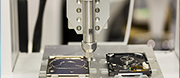
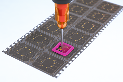
Tagliner Inlay Die Bonder
ADAT3 XF Tagliner is three times faster and 30% more accurate than anything on the market. Common systems only work with transparent web material; this Tagliner handles a diverse range, including paper enabling you to move away from PET plastics for sustainability. Eliminating manual handling through automated wafer change and qualified for die bond of all known ICs down to 200 μm die size, the ADAT3 XF Tagliner performs a complete inspection without sacrificing speed and productivity.
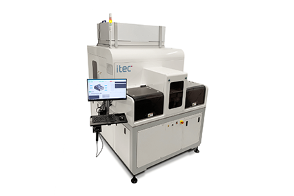
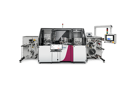
Optical Inspection
ITEC’s AOI family is the best solution for 2nd, 3rd and 4th optical inspection of your production. It also offers mid-end applications for inspection after mold and plating, as well as a full inspection system for chip modules. Inspection can be performed on all the different kinds of products and packages, inline or standalone.
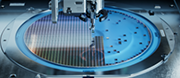
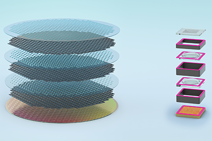
Carrier wafer glass
Used throughout the semiconductor industry, carrier wafers and carrier panels are commonly used to manufacture essential components such as 3D ICs and FO-WLP. In order to withstand the high temperatures required for semiconductor manufacturing, carrier wafers and panels are usually made using a material with high thermal stability. Schott offers a wide range of products with broad CTE range, thickness and different dimension.
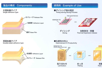
SOMATAC
SOMAR provides thermal heating film for the semiconductor industry, which has been widely used in MLCC cutting. Nowadays, chip sizes are getting smaller and smaller, such as micro-LED and RFID chips. There are always problems, such as chips are difficult to remove and adhesive remains after wafer cutting procedure.